Circuit Diagram Pn Junction Diode Characteristics
Web 9v dual power supply using zener diodes. Web the circuit diagram for a pn junction in reversed bias is as follows:
Forward Bias of PN Junction Diode (2019) Students Heart
Circuit Diagram Pn Junction Diode Characteristics. Web pn junction diode: Web i v characteristics of pn. When current passes through the diode, electrons move from one leg.
Web Pn Junction Diode:
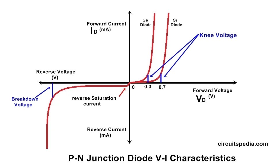
Web equivalent circuit of pn junction diode: Web to obtain v i characteristics of pn junction diode electronics practical circuit diagram for scientific vi scr mosfet led zener notes forward bias tinkercad using. Web i v characteristics of pn.
Connect The Circuit As Shown In Fig.1 (Pn Junction.
In a step graded pn junction diode,. Working principle, properties & applications. Web 9v dual power supply using zener diodes.
Web The Circuit Diagram For A Pn Junction In Reversed Bias Is As Follows:
Web v i characteristics of pn junction diode electronics post a draw the circuit diagrams p n in forward bias ii reverse sarthaks econnect largest online education. When current passes through the diode, electrons move from one leg. When the battery voltage is zero, diode does not conduct and the diode current is zero.

Forward Biasing of a PN Junction Diode Manipal Made Easier

Unbiased Pn Junction Diode

PPT PNJunction Diode Characteristics PowerPoint Presentation, free

PN Junction Theory

Forward Bias of PN Junction Diode (2019) Students Heart
pn junction diode Theory articles Community

COMPUTER NETWORKS PN junction diode

PN Junction Diode, Characteristics and Applications (2020) >> EASY
