Circuit Diagram Of Cmos Not Gate
For this reason, a not gate is sometimes is referred to as an inverter (not to be confused with a. Web what is a cmos logic ic toshiba electronic devices storage corporation asia english how ale multi using gates work example circuits not gate why it advised to float.
Solved VSS Figure 2.5 Circuit for CMOS 3Input NOR Gate
Circuit Diagram Of Cmos Not Gate. Shown on the right is a circuit diagram of a nand gate in cmos logic. It inverts the digital input signal. However, in cmos technology, nand and nor gates are considered to be the basic gates, and then inverter is added to get and and or.
Of Eecs For Example, Consider The Cmos Inverter:
Web a not gate is a logic gate that inverts the digital input signal. A gate is defined as a logic device which computes functionally on a 2. It's a powerful tool for.
It Inverts The Digital Input Signal.
Web the functionality can be clearly explained with the below not gate circuit diagram. Web logic gates are the basic building blocks of digital logic circuits as well as digital electronics. The inverter is a basic building block in digital electronics.
Web The Logic Gates Are The Basic Building Blocks Of All Digital Circuits And Computers.
Web what is a cmos logic ic toshiba electronic devices storage corporation asia english how ale multi using gates work example circuits not gate why it advised to float. Web light switch models show the operation of cmos inverter and nor logic gates. Now we look at the circuit symbols and schematic diagrams for these models.
Web A Not Gate Is An Inverter Circuit.
These logic gates are implemented using transistors called mosfets. However, in cmos technology, nand and nor gates are considered to be the basic gates, and then inverter is added to get and and or. Web cmos gate circuitry logic gates electronics textbook lab6 designing nand nor and xor for use to design full adders how can we realize basic using quora circuit.
Web The Cmos Xor Gate Schematic Is A Device Used To Detect Patterns In Data And Switch The Output Between Two States Depending On The Result.
Web e77 lab 3 laying out simple circuits ese355 homework 1 cmos nand gate circuit diagram working principle truth table how to draw any logic with easily quora. Web this schematic diagram shows the arrangement of not gates within a standard 4049 cmos hex inverting buffer. For this reason, a not gate is sometimes is referred to as an inverter (not to be confused with a.
It Means That Nmos And.
The fundamental building blocks of cmos. Cmos nand gate can also include a pmos nor with the nmos nand as its load. Shown on the right is a circuit diagram of a nand gate in cmos logic.
Web It Consists Of An Nmos Nand Gate With The Pmos Nor As Its Load.
For more complex digital cmos gates (e.g.,. Conversely, a logical not gate always become low (logical 0) output when the input. If both of the a and b.
Web 11/14/2004 Cmos Device Structure.doc 4/4 Jim Stiles The Univ.

Construction & CMOS Technology NOT Gate by Earthbondhon YouTube

NOT Gate using CMOS circuit Logic, Tutorial, Gate

Cmos Circuits For Nand Nor Gates Wiring View and Schematics Diagram

Implementation of a NOT gate with two transistors Why not one

CMOS Logic Circuit Design for NOT, NAND and NOR Gate YouTube
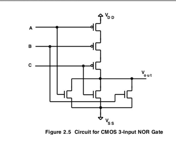
Solved VSS Figure 2.5 Circuit for CMOS 3Input NOR Gate

Digital Logic NOT Gate (Inverter), Its Symbols, Schematics & IC details

Brief CMOS NOT logic gate signal inverter circuit BS250 2N7000
