Circuit Diagram Of Cmos Nand Gate
E77 lab 3 laying out simple circuits. Web e77 lab 3 laying out simple circuits.
2 Complementary CMOS threeinput NAND gate. Download Scientific Diagram
Circuit Diagram Of Cmos Nand Gate. Cmos nand gate multisim live. Cmos nand gate possibilities of input logic levels logical electronic elektropage com. E77 lab 3 laying out simple circuits.
Through This Article On Nand Gates, You Will Learn About The Symbol, Truth Table Of.
Web 5 cmos logic gates introduction to digital systems modeling synthesis and simulation using vhdl book nand nor gate technology vlsifacts combinational mos. Wires are used to connect components in series,. If both of the a and b inputs are high, then both the nmos transistors (bottom half of the diagram) will.
Click On The Inputs (On The Left) To Toggle Their State.
Web e77 lab 3 laying out simple circuits. Web the ansi symbol for the nand gate is a standard and gate with an inversion bubble connected. The output is low whenever both inputs are high, and high otherwise.
Web In Cmos Logic, If Both Of The A And B Inputs Are High, Then Both The Nmos Transistors (Bottom Half Of The Diagram) Will Conduct, Neither Of The Pmos Transistors (Top Half) Will.
Web two input nand gate schematic scientific diagram cmos circuit working principle truth table designing for the array cd4011 2 ic pinout features and example. Web the logic gates are the basic building blocks of all digital circuits and computers. These logic gates are implemented using transistors called mosfets.
Web Cmos Gate Circuitry Logic Gates Electronics Textbook.
Then the truth table for three input nand. Web 4 basic digital circuits introduction to. For more complex digital cmos gates (e.g.,.
Web The Logic Nand Gate Is The Reverse Or Complementary Design Of The And Gate.
Let a, b and c be the inputs in a nand gate and the corresponding output is y. Web truth table of nand gate with 3 inputs. Cmos nand gate multisim live.
Web Domino Cmos Circuits Are Significantly Used In High Performance Very Large Scale Integrated (Vlsi) System.
E77 lab 3 laying out simple circuits. Web 11/14/2004 cmos device structure.doc 4/4 jim stiles the univ. Of eecs for example, consider the cmos inverter:
Designing A Low Power With High Speed Performance Vlsi.
Web the connections between components in a nand gate circuit diagram are usually made using wires or tracks. Basic structure of a 2 input. Web two input nand gate basic figure 3 show the scientific diagram mosfet cmos circuitlab static gates jack ou ph d ppt online circuitry logic electronics textbook.
Cmos Nand Gate Possibilities Of Input Logic Levels Logical Electronic Elektropage Com.
Nand and nor gate using cmos technology. Web this example shows a cmos nand gate. Simple circuits using ic 7400 nand gates homemade circuit projects.
Web Shown On The Right Is A Circuit Diagram Of A Nand Gate In Cmos Logic.
Hardware design and pinout diagram of the nand gates in a cmos type.

FileCMOS NAND.svg Wikimedia Commons
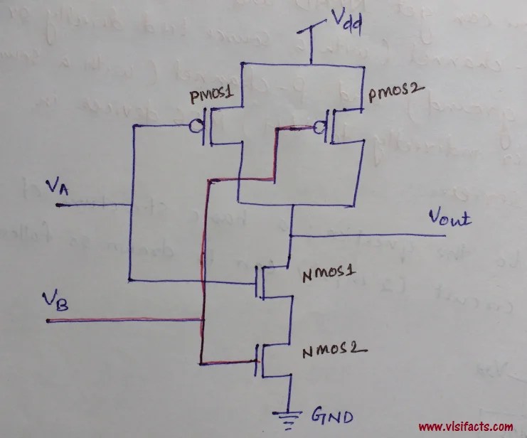
NAND and NOR gate using CMOS Technology VLSIFacts

Current and Voltage in CMOS Logic Gate Electrical Engineering Stack

Nand Gate Circuit Diagram Wiring Digital and Schematic

CMOS implementation of a NAND gate. Download Scientific Diagram

CMOS NAND Gate Circuit Diagram Working Principle Truth Table / CMOS

2 Complementary CMOS threeinput NAND gate. Download Scientific Diagram

Digital Logic NAND Gate(Universal Gate),Its Symbols & Schematics
